


Entrepreneurial Support Program(Explore Course)


- Principal Investigator
-
The University of Tokyo
Junichiro Kadomoto
- Adopted Theme
Ultra-High-Speed, Ultra-Low-Latency Wireless Isolated Communication Technology for SiC/GaN Power Electronics
- Subject of Research
- Ultra-High-Speed, Ultra-Low-Latency Wireless Isolated Communication Technology for SiC/GaN Power Electronics
- GTIE VC Collective
Advanced Technology Acceleration Corporation (ATAC)
- Overview
-
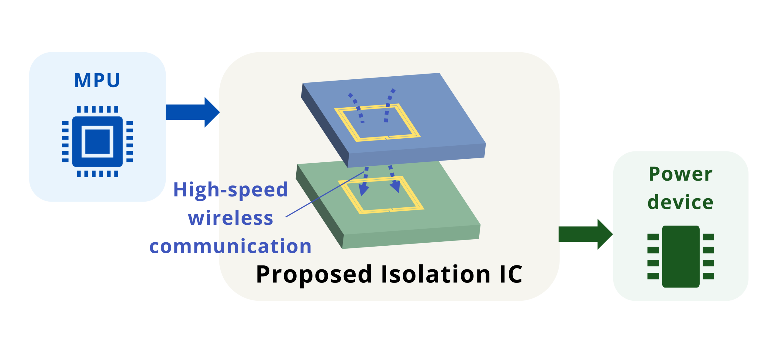
With the spread of physical AI, including humanoid robots, motor control and power control that operate accurately and safely in the real world are becoming increasingly important. In power electronics, where SiC/GaN power devices are being adopted more widely, switching speeds are approaching the nanosecond level, and the ability to transmit control and sensor signals across an isolation barrier with low latency has become a key enabling technology for equipment performance. Existing photocouplers and digital isolators, however, are generally limited to Mbps-class data rates and cannot meet this requirement. This project applies a proprietary wideband on-chip coil structure and a simple baseband communication scheme to signal transmission across an isolation barrier, and develops a next-generation isolation IC that achieves both Gbps-class ultra-high-speed communication and sub-5-ns ultra-low latency. By further integrating the isolation function with ADCs, amplifiers and drivers into multi-chip devices, the project builds an isolation semiconductor platform and aims to establish a startup targeting the global market.
- Business Models(when applying)
The business targets manufacturers of power electronics equipment and adopts a fabless model in which isolation ICs are designed and sold as semiconductor components. Initial products focus on applications where ultra-high-speed, ultra-low-latency transmission delivers direct value, such as active gate drivers. The product line is then expanded to higher value-added multi-chip devices that integrate the isolation function with ADCs, amplifiers and drivers. Licensing of intellectual property covering the proprietary coil structure and communication scheme is also positioned as a revenue stream.
- Activity Planning(when applying)
From FY2026 to FY2029, the project advances in stages from technical proof of concept of the isolation chip to preparation for company formation. In R&D, the first year defines the required specifications such as data rate, propagation delay, jitter, noise immunity and isolation voltage, and completes the chip design. The second year covers fabrication. The third year covers device-level characterization and multi-chip operation testing using an evaluation board. The fourth year covers comprehensive evaluation in the multi-chip configuration. The target performance is Gbps-class data rates, sub-5-ns propagation delay, CMTI of 200 kV/μs, and 3 kVrms-class isolation. In business development, customer interviews, competitive benchmarking and IP strategy planning begin in the first year, followed by the search for PoC partners, patent filings and business planning. The third year establishes the management structure together with the financial and capital policy, and the fourth year covers international expansion planning and the establishment of the startup.